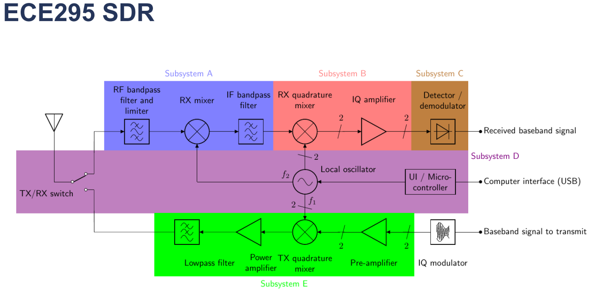
Design
Preface
To prevent future students from copying my design
(and to avoid an appearance before the UofT Tribunal
for an academic offence),
all circuit element values and calculations are omitted from
this website.
If you are curious to see the design files and
calculations,
contact me ![]() directly :)
directly :)
Subsystem C: Design Requirements
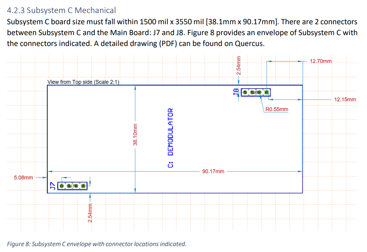
The following is a list of requirements that our design had to meet. We had to interface with Subsystem B and the board also had to fit within set dimensions to be placed on the SDR motherboard.
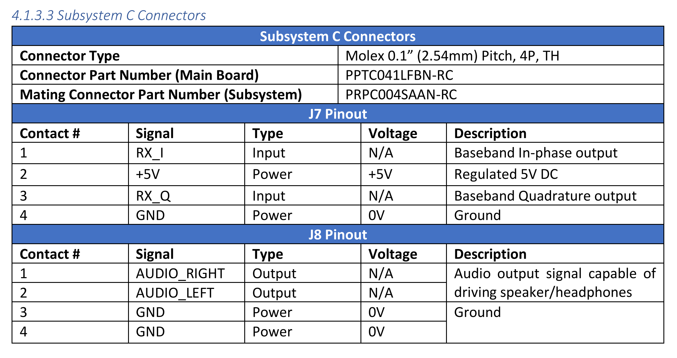
- 2 input signals: Baseband I (in-phase) and Q (quadrature) signals from Subsystem B
- AM input signal specification: 40 - 100kHz carrier frequency, 20Hz - 3kHz message signal
- SSB input signal specification: 2 - 3kHz carrier frequency, 0 - 3kHz message signal
- 1 duplicated output signal for two 8Ω speakers (mono)
- Switching between AM and Single-Sideband (SSB) Demodulation + volume control
- SSB phase specification: I and Q must be set 90° ± 12.5° apart
What does it all mean?
Honestly, most of these requirements didn't make sense when I saw
them for the first time. Later on, I realized that a lot of the concepts
we'd apply to our designs were actually taught in third-year,
but the teaching team helped us learn
quickly enough to design our board.
That help came after the first design review, where we learned just how
much was wrong with our first design.
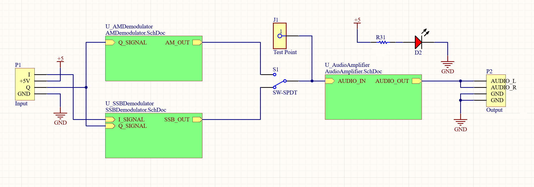
First Revision
I know this is a lot to look at initially, but I wanted to show how disorganized our first revision was because we put everything on the same schematic. Right off the bat, there were two mistakes, but we wrung out almost all of our issues by the second design review.
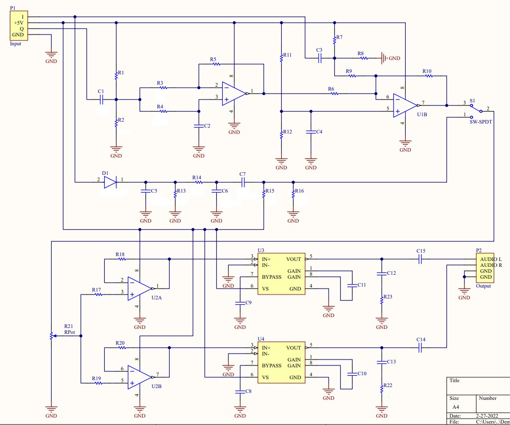
SSB Demodulator - The First Problem
Multisim Outputs: Red - In-Phase, Green - Quadrature, Blue - Summed Audio Output
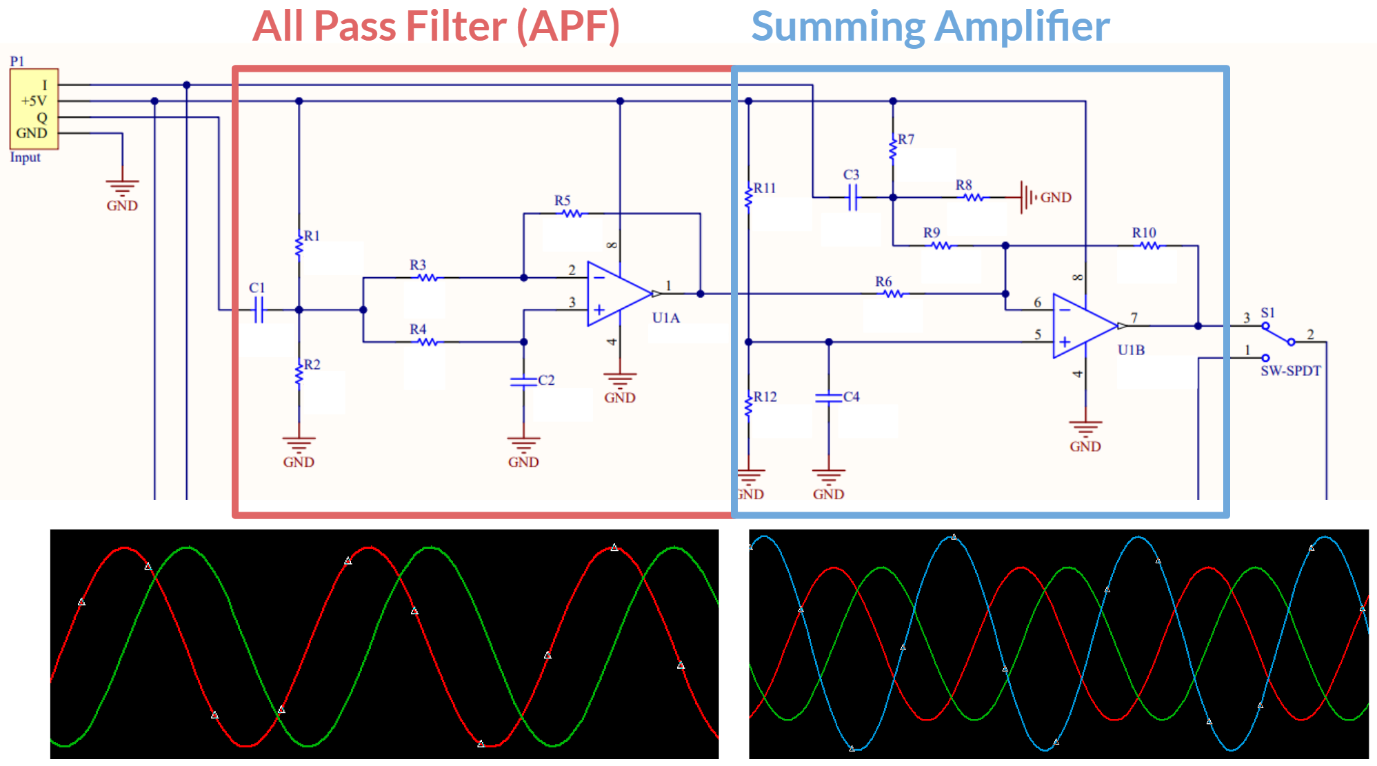
Before moving into what's wrong with this design, I'd like to mention one thing we
did right—op-amp biasing. The motherboard only supplied us with 5V and GND
terminals, meaning our signals had to be centred at 2.5V to make use of the op-amps.
If you look at the C1-R1-R2, C3-R7-R8 and C4-R11-R12 combinations, they centre the
input signals and the op-amp positive terminal in U1B. We made sure the cut-off frequency
of the resistor and capacitor combinations was high enough to allow our signals to pass
through.
As for the problem, it has to do with the first op-amp. In SSB Demodulation, the
I and Q signals are shifted 90 degrees apart and then added together.
This gives us an audio signal at the output terminal of the second op-amp. The first op-amp
is an All-Pass Filter (APF) that shifts the Q signal by 90 degrees, and the second op-amp is
a Summing Amplifier that adds the two signals together.
The issue was that the APF only shifted 10kHz signals by 90 degrees, rather than a
range of frequencies. Even if the SSB signal was centred at 10kHz, the message signal (audio)
ranges from 0 - 3kHz on top of that, which would have given us an improper phase shift.
The summing was done right, even though it's an inverted (audio) signal. Audio can be upside
down, or you'd hear something different when you put your headphones on upside-down.
AM Demodulator - No Issues
Multisim Outputs: Red - AM Signal, Green - Envelope, Blue - Audio Output
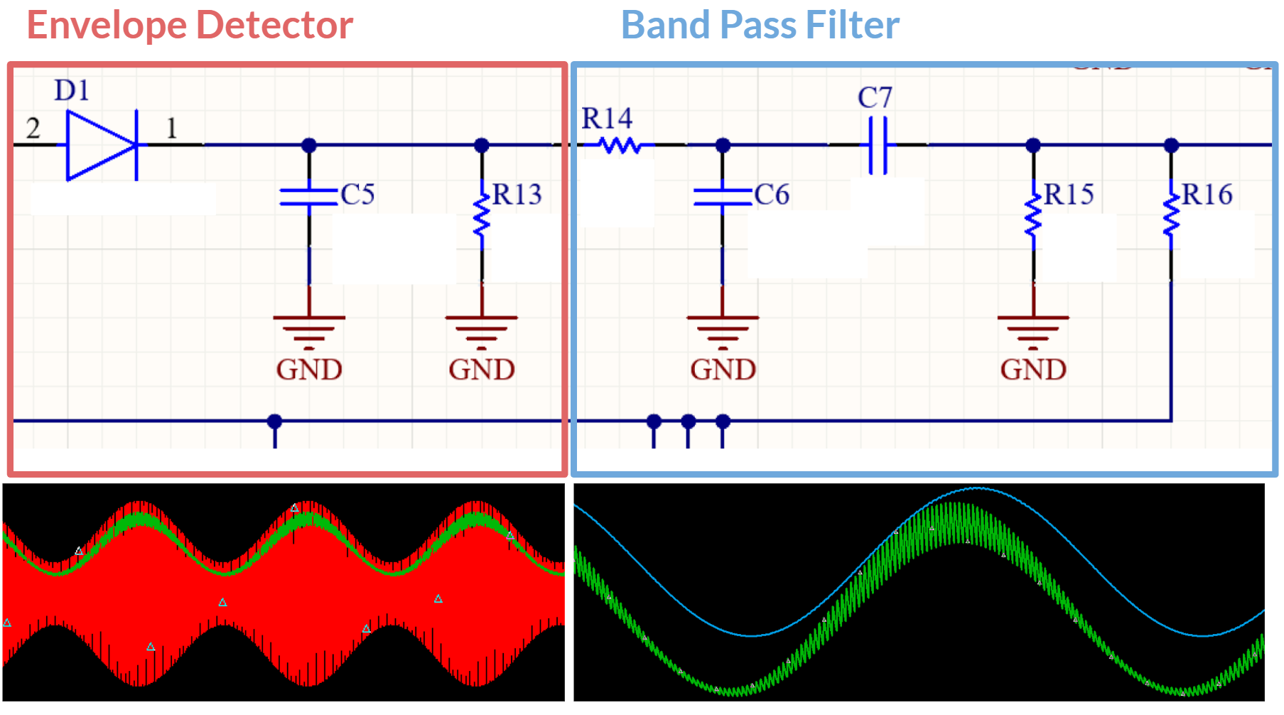
In AM Demodulation, the Amplitude-Modulated (AM) signal is first passed through an
Envelope detector which traces the amplitude of the signal with less perturbation.
Then that signal passes through a Band-Pass Filter (BPF) which further smoothens out the signal,
leaving us with a filtered audio signal. There's a formula for the R13-C5 combination that we
used to make sure it optimally envelopes the 40kHz - 100kHz AM signal.
The C7-R15-R16 combination was to bias the signal at 2.5V, to centre it for the op-amps
ahead of it (which were ultimately redundant, scroll down to read more). Typically an
AM Demodulator has only a Low-Pass Filter, but the biasing turned it into a BPF in our initial
design.
Unity Gain Buffers and Audio Amplifiers - The Second Problem
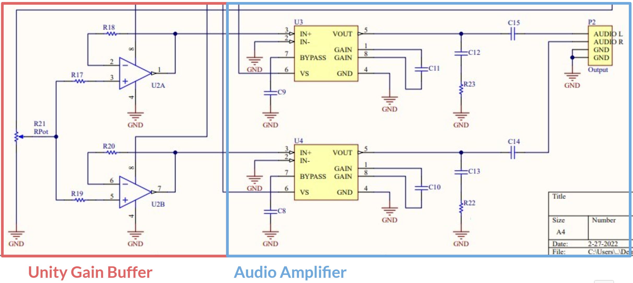
We thought we'd need Unity Gain Buffers (UGB) to duplicate the audio signal without loss. We were wrong. Turns out a single audio amplifier chip was enough to amplify the signal for both left and right audio channels (there's adequate impedance at the input and output terminals of the chip), so we were able to remove 75% of the components in this part of the design. The UGBs weren't AC coupled with a capacitor to the audio amplifier chips, so that was another issue we overlooked in our first iteration.
Second Revision
A few weeks later, we had our second design review. We showcased an organized design for our board to the teaching team which had far fewer issues. We added a test point between the demodulators and the audio amplifier, which is the perfect point to test all three systems independently with a single reference point. We also implemented an LED indicator light to avoid having to check for power every time we tested the circuit.
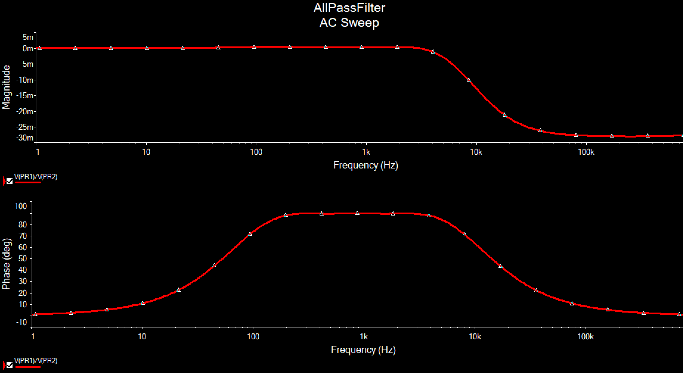
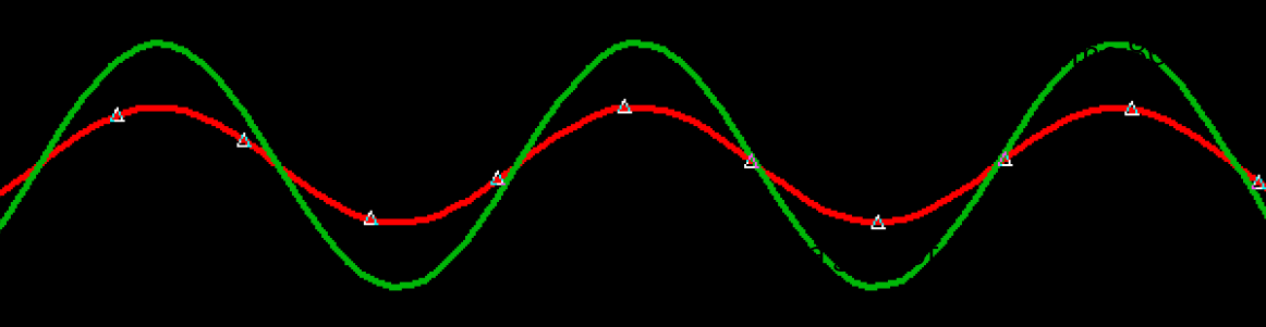
The Improved SSB Demodulator
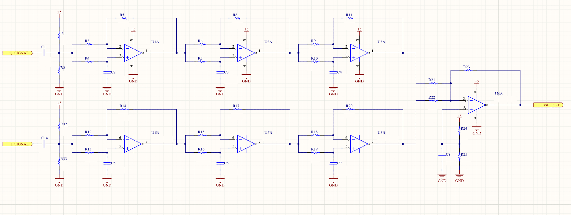
This time a chain of three APFs for both input signals was used. We found a reference design that was provided by the TA to help us choose our element values, which creates a clean range of 90-degree phase shifting between 250Hz to 3.6kHz as you can see in the output graph. The Summing Amplifier was not modified.
Modifying the AM Demodulator
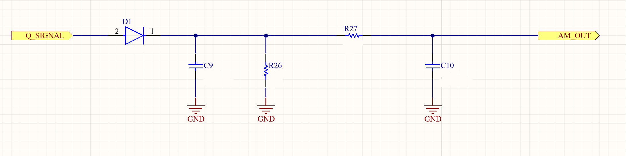
Not much changed here apart from removing the 2.5V biasing, since we didn't have UGBs anymore. We tweaked the RC values a little to optimize more for a 0 - 3kHz message signal.
The Simplified Audio Amplifier
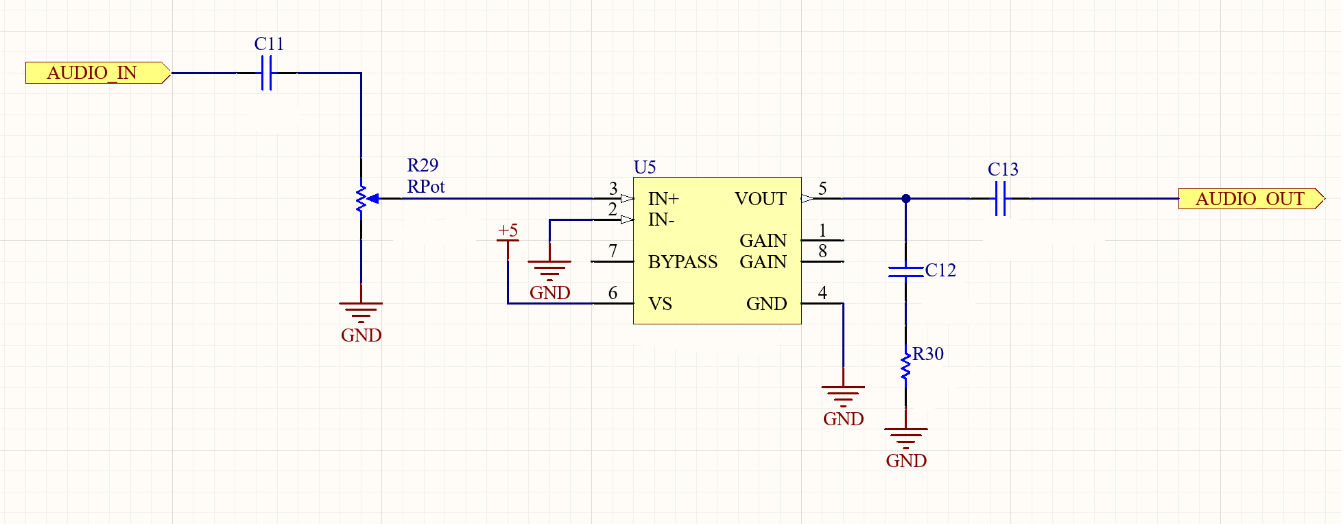
Since the second Audio Amplifier and the UGBs had been removed,
the design became a lot simpler. We also added C11, which AC couples the demodulators
(mainly the SSB since it is sending a signal biased to 2.5V) to the amplifier.
We had a minor issue with this design which was never solved. Since we only had
a 5V supply, the amplifier would clip the audio if we set the volume too high with the
potentiometer. Ultimately we used a higher resistance potentiometer which made our
design capable of 65% volume before clipping.
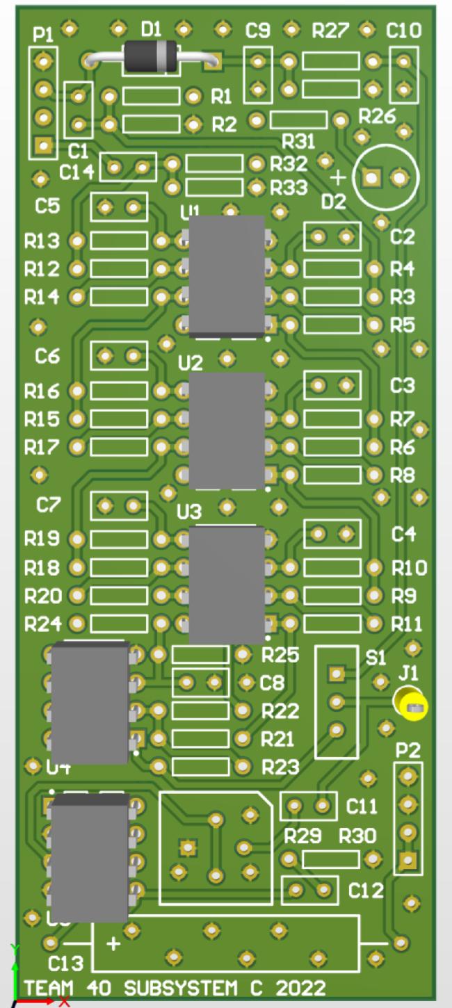
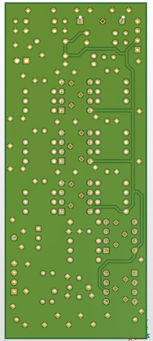
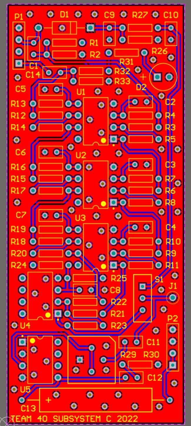
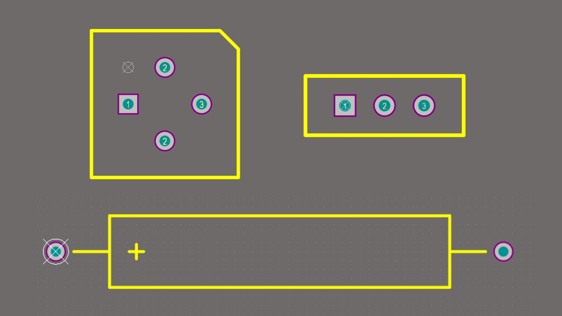
PCB Design
A week after the second design review, our PCB Designs were due for review
(as well as circuit reviews for teams that needed to tweak their design more).
It was challenging to fit everything on such a small board, so I spent
the entire week avoiding my other courses to arrange our design as best as
possible and ordering parts. I could have chosen to place all the resistors in a
hairpin style, but I wanted to make sure our design followed good practices. It
was also my favourite part of the project and I was very satisfied with the
PCB arrangement :)
The subcircuits are distinguishable on the board. The five elements connected at the top
make up the AM Demodulator, and beneath it is the LED indicator. Then most of the board
is taken up by the SSB Demodulator (elements connected to U1 - U4). You can see both the
demodulator outputs connected to S1 near the bottom right, right next to the J1 test point.
Lastly, at the bottom of the board, is the Audio Amplifier.
All signal traces were on the top plane (red), while the 5V power signal was on the bottom plane (blue).
In terms of good practice, I also placed ground planes on both the top and bottom.
We didn't go into the details of EM shielding, but for safe measure, I added via stitching between
the two ground planes.
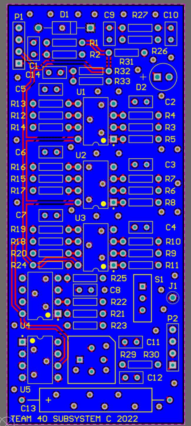
Designing Footprints
Our volume potentiometer, audio output capacitor and SPDT switch didn't have footprints available online, so I made their footprints myself following their datasheets. In the case of the potentiometer, the datasheet didn't clearly specify which turn direction increased the resistance between pin 2 and 3, so I included two pin 2 nets in the footprint so that I could flip the potentiometer to achieve a clockwise volume increase. Once the potentiometer arrived, we determined that the correct position for clockwise volume increase (or resistance decrease) was to use the top pin 2 position.
What next?
Once we double checked that we passed both the ERC and DRC, the PCB was ready to be manufactured. It took nearly a month for the boards to arrive, but in the meantime, we tested a prototype of our design. Even though prototyping was not mandatory for the project, it was a necessary step to check for issues in case our PCB didn't work on the first attempt.